

In this modern era, smartphones have completely rewritten the rules of photography, driving traditional compact digital cameras to near-extinction. Yet, even though we carry these devices in our pockets every single day, how many of us truly understand the intricate optical clockwork sealed within those razor-thin chassis? Looking at the flat, flush back of a modern smartphone, a pure enthusiast might naturally wonder: "Is there actually a real lens architecture hidden inside here?"
In this article, we conduct a rigorous, reverse-engineered technical review of the Apple iPhone wide-angle camera system. By extracting design data from official patent literature, reconstructing the optical path inside our simulation software, and evaluating its aberrations, spot diagrams, and MTF, we unveil the raw, unadulterated performance of this everyday marvel.
Crucially, this analysis extends beyond mere theoretical equations. We also explore the groundbreaking manufacturing ecosystem that turned these blueprints into physical reality—specifically looking at how industry leaders like Taiwan's Largan Precision mass-produce these ultra-precise components. Welcome to a deep-dive analysis you won’t find anywhere else on the internet.
1. Patent Literature Context & Identification
To evaluate the core optical DNA of modern smartphone cameras, we trace the foundational engineering back to Apple’s extensive patent portfolio. Specifically, this analysis is built upon the design data disclosed in US Patent Application US2017/0299845.
This foundational patent centers on an advanced optical configuration specifically engineered to mitigate internal reflections—commonly recognized as "ghosting"—within the ultra-compact lens assembly. The patent application presents multiple design examples. For this deep dive, we have extracted the raw mathematical prescriptions from Embodiment 1 , which details a highly sophisticated 6-element (6P) architecture with a focal length and aperture specification equivalent to 28mm f/1.8 (when proportionally scaled). Based on the timeline and the specific optical parameters, it is highly reasonable to infer that this design closely mirrors the actual lens design implemented during the iPhone 8 generation.
By inputting the official radii of curvature, axial distances, refractive indices , Abbe numbers , and high-order aspherical coefficients (extending up to the 14th and 16th orders) into our optical simulation software, we have perfectly resurrected the exact design intent of Apple’s optical engineering team.
2. Lens Specifications & Scaling Philosophy
A critical challenge when reviewing smartphone optics is the massive scale disparity compared to traditional photographic lenses. A smartphone image sensor is incredibly small, typically utilizing a 1/3-inch format with an image circle diagonal of approximately 6.0 mm. If we analyze its aberrations natively, the absolute geometric values appear misleadingly superior simply due to the tiny scale.
To maintain a fair, logical baseline across all reviews on LENS Review, we have applied a proportional scaling factor (approx. 7x) to longitudinal dimensions. This projects the lens performance onto a standard 35mm Full-Frame baseline. In short, the data below answers the ultimate question: "How would this iPhone lens perform if it were physically magnified to Full-Frame dimensions while maintaining its native angles of incidence?"
| Optical Parameter | Native Prescriptions (1/3" Sensor) | Full-Frame Equivalent (Scaled) |
| Focal Length (f) | approx. 4.1 mm | 28 mm |
| Aperture Ratio | $f/1.8$ | $f/13$ (Depth-of-field equivalent) |
| Lens Configuration | 6 elements in 6 groups (6P, All-Plastic Injection) | 6 elements in 6 groups (6P, All-Plastic Injection) |
| Total Track Length (TTL) | approx. 5.5 mm | - |
| Aspherical Profile Count | 12 surfaces total (100% fully aspherical) | 12 surfaces total (100% fully aspherical) |
3. Cross-Sectional Optical Path & Structural Marvel
The layout features an ultra-compressed 6-element-in-6-group configuration. For anyone accustomed to looking at large glass elements for mirrorless systems, this cross-section is an absolute shock to the system. Six distinct plastic elements are stacked within a total mechanical depth of just 5.5mm, including the cover glass and infrared cut-off filter (IRCF).
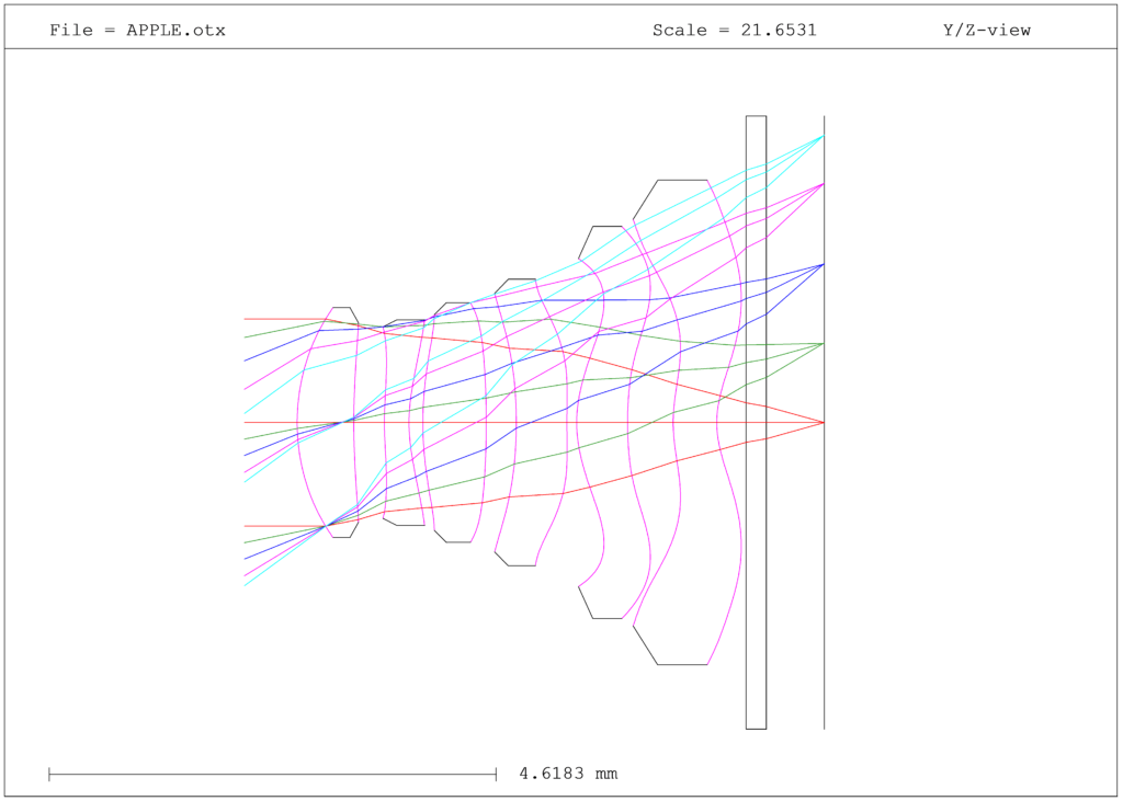
The geometry of the 5th and 6th elements—the surfaces closest to the image sensor—is profoundly radical. Their shapes exhibit intense, undulating inflection points that resemble a wave or a gull-wing profile. To readers of my generation, the silhouette of that 6th element immediately evokes the iconic "Eye Slugger" (the crest blade) from the classic tokusatsu series Ultra Seven—though that reference might fly completely over the heads of our Gen-Z audience!
Pop-culture humor aside, this extreme geometry is absolutely vital. Its role is to aggressively bend off-axis rays, ensuring they strike the sensor at an angle close to perpendicular, thereby minimizing pixel-level vignetting caused by the sensor's micro-lens structure.
4. Comprehensive Aberration Analysis
Let us delve into the core scientific data. To evaluate the raw geometric precision, the aberration characteristics plotted below have been scaled completely to Full-Frame equivalence.
Spherical Aberration
Despite operating at a remarkably fast native aperture of $f/1.8$, the spherical aberration is corrected to an astonishingly low level. In traditional interchangeable camera lenses, integrating two or three aspherical surfaces is deemed a high-end luxury. In this smartphone module, however, every single one of the 12 surfaces is aspherical. Each surface operates as a precise mathematical variable, suppressing high-order spherical errors before they can accumulate. The resulting curve on our chart shows a nearly vertical profile near the optical axis, signifying excellent central contrast.
Axial Chromatic Aberration
Because this lens operates without a physical iris diaphragm—meaning it is mechanically locked to shoot strictly wide-open at $f/1.8$ at all times—axial chromatic aberration must be managed entirely through material selection. By meticulously pairing high-dispersion polymers with low-dispersion polymers (the plastic equivalents of crown and flint glass), the secondary spectrum is tightly bounded. While a small amount of residual color separation between the $g$-line (blue) and $C$-line (red) is visible under high magnification, it remains exceptionally well-controlled for an all-plastic optical train under 6mm in total length.
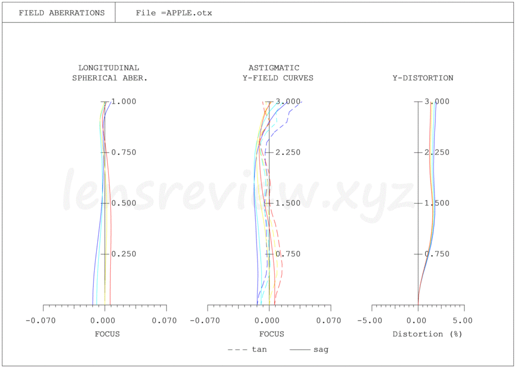
Field Curvature
When examining the astigmatic field curvature, the Sagittal (S) and Tangential (T) planes remain beautifully synchronized up to the mid-field. Near the extreme periphery, however, the curves exhibit a characteristic wave-like flare. This is a direct consequence of the aggressive higher-order aspherical coefficients working overtime to force off-axis rays onto the flat sensor plane. For a wide 28mm equivalent field of view compressed into such a short optical track length (TTL), this level of flatness across the main imaging area is highly impressive.
Distortion
The native optical distortion plotted from the patent values reveals a significant amount of barrel distortion (approaching several percent when uncorrected). If you were to shoot a straight grid with the raw optical module, the lines would curve inward dramatically.
However, this is completely invisible to the end user due to a hybrid architecture: Optical-Digital Co-design. Modern smartphone cameras capture a wider native field of view than advertised, and the internal image processor (ISP) applies a real-time coordinate mapping algorithm to stretch and flatten the image into a perfect, distortion-free 28mm perspective. This paradigm shift proves that physical space constraint is the ultimate enemy; why waste precious millimeters of thickness correcting distortion optically when silicon can do it instantaneously?
Lateral Chromatic Aberration
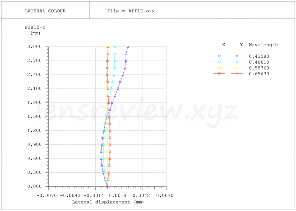
Looking at the lateral chromatic aberration (chromatic aberration of magnification), our simulation reveals a distinct, progressive separation of color wavelengths toward the extreme corners of the frame. In traditional full-frame lens design, this would be highly penalized.
However, in smartphone optics, leaving a predictable amount of lateral chromatic aberration uncorrected is a calculated, strategic choice. Because this aberration does not reduce the core contrast but merely shifts the registration of color channels linearly, it can be perfectly corrected via software algorithms within the ISP pipeline during raw conversion. By offloading this task to digital processing, Apple's engineers successfully avoided adding extra weight or thick compensating elements to the physical module.
Lateral Aberration
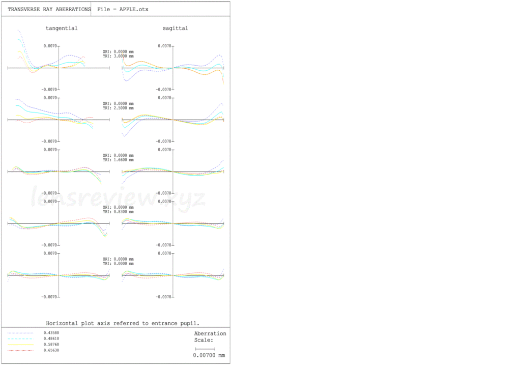
The transverse/lateral aberration plots provide a microscopic look at ray behavior across the frame. At the center, the ray intercept curves are nearly flat, confirming a highly coherent wavefront. As we move off-axis toward the mid and maximum field heights, we can observe the emergence of asymmetrical coma and high-order aberrations that correspond to the peripheral wave seen in the field curvature. Given that these rays are being bent by ultra-thin plastic surfaces separated by mere fractions of a millimeter, keeping the ray scatter within these boundaries is a spectacular achievement in optical computing.
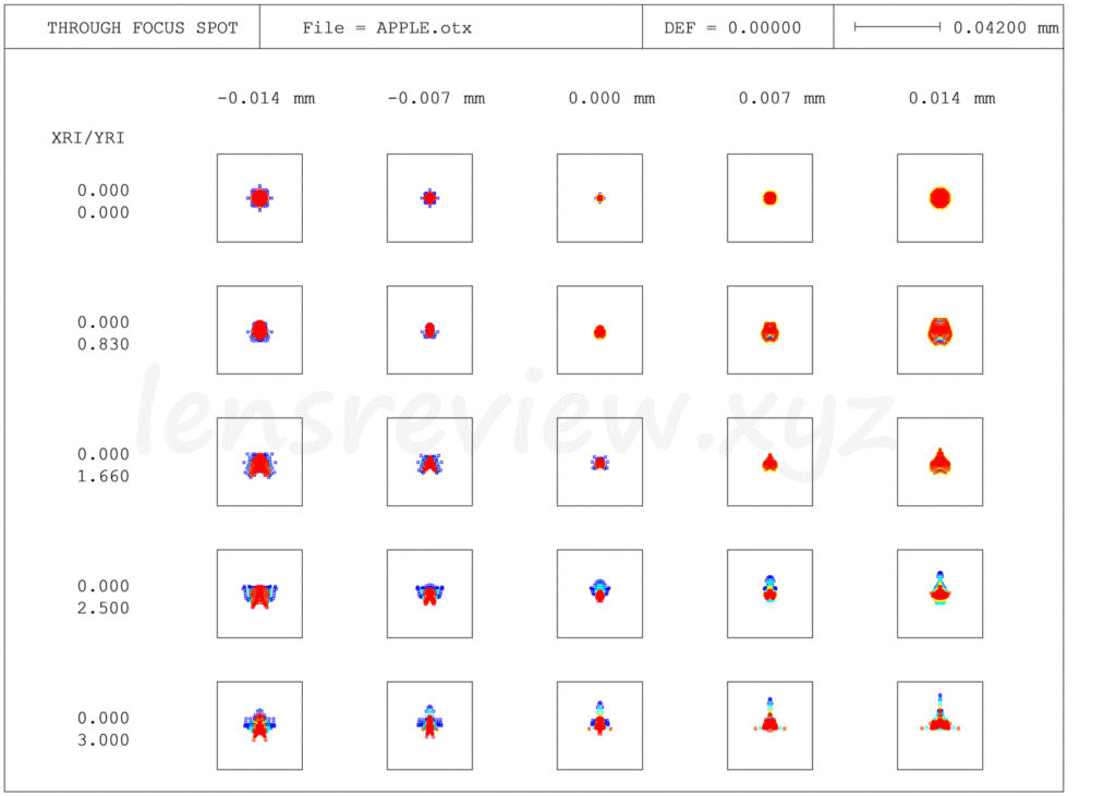
5. Spot Diagram Analysis & Image Circle Quality
To fully grasp the geometric distribution of light rays across the sensor plane, we analyze the spot diagrams across multiple field points. In accordance with the long-standing evaluation protocol of our consortium, the charts are presented using two distinct resolution scales to ensure a completely unbiased look at performance:
Standard Scale (0.3mm adjustment): Used to evaluate the macro-level geometric distribution of rays across the entire image circle.
Detail Scale (0.1mm adjustment): A high-magnification view used to inspect the central core intensity and micro-contrast capabilities.
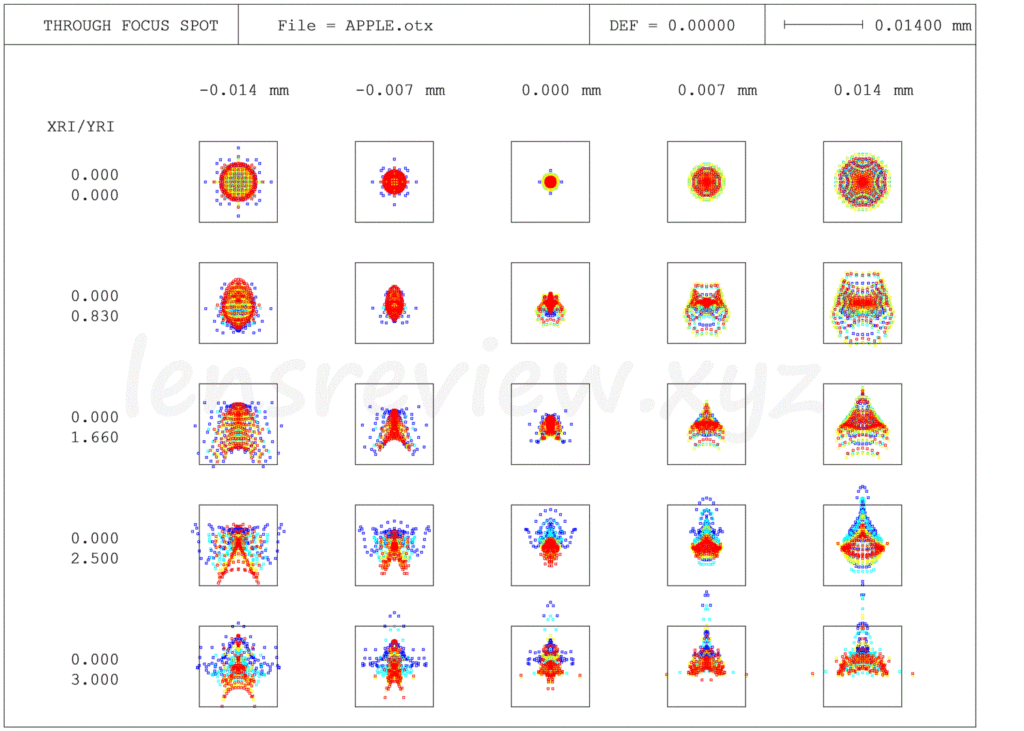
The resulting charts are a masterclass in modern polymer optimization. On the Standard Scale (0.3), the overall ray scatter is tightly contained within the evaluation boundary across almost the entire field. Switching to the high-magnification Detail Scale (0.1), we can observe that at the absolute center, the spot forms a beautifully concentrated, dense point source with almost no flare.
As we march out to 70% and 100% field heights, the spots deform into a characteristic "winged" coma shape—resembling a tiny bird spreading its wings. Yet, given that these rays are being bent by ultra-thin plastic surfaces separated by mere fractions of a millimeter, keeping the spot core this tight is a spectacular achievement in optical computing.
6. MTF (Modulation Transfer Function) Performance
Following our spatial evaluation, the MTF chart provides the final numerical verification of this lens's resolving power. When evaluated at spatial frequencies calibrated to the ultra-fine pixel pitch of modern smartphone sensors, the performance curves tell a fascinating story.
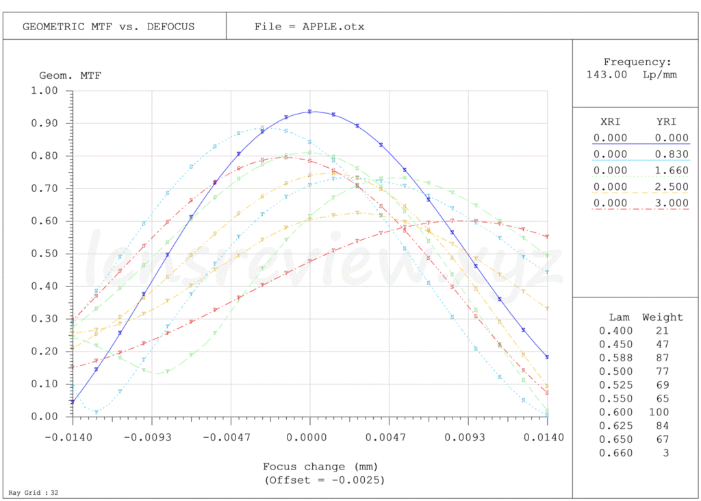
At the center of the frame (0mm field height), the MTF curve stays remarkably high, clinging close to the theoretical diffraction limit. This explains why fine text and central subjects look incredibly crisp in iPhone photos. However, as we move out to the mid-field and extreme corners, we observe a clear separation between the Sagittal and Tangential curves—a classic indicator of the residual astigmatism and coma captured in our lateral aberration analysis. While the contrast drops slightly in the extreme corners, the overall uniformity is exceptionally high for a wide-angle system operating wide-open at $f/1.8$.
Conclusion: The Triumph of Computational Plastics & Manufacturing Mastery
Decades ago, serious photographers laughed at the concept of "plastic lenses," associating them purely with disposable toy cameras like the legendary Utsurundesu (QuickSnap). Today, Apple’s 6P architecture turns that old hierarchy completely on its head.
However, we must remember that designing an incredible optical blueprint in a simulator is only half the battle. Bringing a 12-surface, fully aspherical all-plastic architecture into physical reality requires an almost impossible level of manufacturing precision. This is where the supply chain supremacy of Largan Precision comes into play. By leveraging ultra-advanced plastic injection molding technology, Largan successfully mass-produces these microscopic elements with nanoscale surface tolerances, making high-performance smartphone photography accessible to billions of users worldwide.
Furthermore, patent US2017/0299845 proves how deeply these engineers analyzed structural ghosting reduction, ensuring clean image acquisition even in demanding back-lit scenarios. It is a brilliant marriage of raw optical physics, supply chain mastery, and modern digital processing—proving that the best lens in the world might just be the one that is already inside your pocket.